PCB panel design
Closed, ResolvedPublic

Description

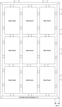
Create a custom PCB panel (gerber) with several subpanels of 3x3 grid of several PCBs (we need the same number of each board, only plugin modules/shields can be different number as those are optional for customers)

  • Add CNC routes for board separation
  • No mousebites for PCBs in grid in subpanel (just CNC routing for separation)
  • mousebites for subpanel separation
  • Add subpanel labels (text)
  • subpanels should be around 20x35cm (squegee is 350mm wide, suggested 345mm paste area max) - the transport belt can be adjusted but more than 200mm width is not recommended as the boards bend to much if wider.
  • 5mm strips for transport belt at the long sides of subpanels
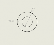
  • 2 diagonally positioned fiducials (ideally asymmetrical to the print contour) per print side with SMT placement. Circle Copper diameter 1.20mm, silkscreen diameter: 2.30 mm.
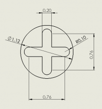
  • Origin: Preferably as a cross in a corner on the top of the print (no solder resist). For SMT placement also on the bottom side of the print (in this case the two origins must lie directly above each other).
  • subpanel dimensions: min. 50 x 50 mm, max. 345x200mm
  • subpanel should have 4 holes near the corners for being held in place during CNC milling (board separation) - 2 or 3mm diameter

Reference:

Todos:
☑ Add subpanel fiducials (Tele requirement: Diameters Cu=1.20mm ; Silkscreen=2.30 mm) 3 layers involved: copper in the middle, solder mask removed around the copper (larger diameter) and silk screen marking (even further out)
☑ Add subpanel origin (Preferably as a cross in a corner on the top of the print (no solder resist). For SMD placement also on the bottom side of the print - in this case the two originals must lie directly above one another)
☐ Add subpanel CNC bridges
☐ Add panel mousebites
☐ Add panel Label
☑ Add subpanel label

Origin (cross = copper; circle = soldermask):

Fiducial:
Related Objects

StatusAssignedTask
ResolvedBAndiT1983
ResolvedBAndiT1983
BAndiT1983 moved this task from Backlog to PCB on the AXIOM Beta Hardware board.
sebastian updated the task description. (Show Details)May 11 2020, 10:56 PM

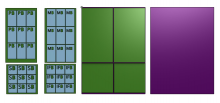
This was supplied as output by manual panellization in altium

The chiprow above the actual Panel is to be ignored.

sebastian updated the task description. (Show Details)May 11 2020, 11:17 PM
sebastian updated the task description. (Show Details)May 11 2020, 11:22 PM
sebastian updated the task description. (Show Details)May 11 2020, 11:31 PM
sebastian updated the task description. (Show Details)
sebastian updated the task description. (Show Details)May 11 2020, 11:33 PM
sebastian updated the task description. (Show Details)May 11 2020, 11:36 PM
sebastian updated the task description. (Show Details)
sebastian added a comment.EditedMay 12 2020, 10:54 AM

Example gerber package sent to PCB manufacturer (single PCB, no panel).

This is an Eagle CAM job export (oshpark 4 layer standard).

sebastian updated the task description. (Show Details)May 30 2020, 4:53 PM
sebastian updated the task description. (Show Details)
sebastian updated the task description. (Show Details)May 30 2020, 5:05 PM
sebastian added a comment.EditedMay 31 2020, 3:08 PM

subpanel separation mouse bit design:

sebastian updated the task description. (Show Details)Jun 21 2020, 1:20 PM
sebastian updated the task description. (Show Details)Jun 21 2020, 1:27 PM
sebastian updated the task description. (Show Details)
sebastian updated the task description. (Show Details)Jun 21 2020, 1:35 PM
sebastian updated the task description. (Show Details)Jun 21 2020, 1:50 PM
sebastian updated the task description. (Show Details)Jul 2 2020, 9:21 PM

new repo has been created and we started filling it: https://github.com/apertus-open-source-cinema/pcb-paneliser

sebastian updated the task description. (Show Details)Jul 2 2020, 9:30 PM
sebastian updated the task description. (Show Details)Jul 2 2020, 9:35 PM
sebastian updated the task description. (Show Details)Jul 5 2020, 2:53 PM
sebastian closed this task as Resolved.Jul 31 2020, 9:38 AM
sebastian added a subscriber: Bertl.

Excellent job @BAndiT1983 , I think for now all open subtasks have been completed!

sebastian reopened this task as Open.EditedSep 28 2020, 11:41 AM

New issues to resolve:

KiCAD complains about macros when opening stage 1
RS274X: Aperture Macro "MACR": Invalid primitive id code 90, line 12: "1,0,$3,0,0,90*% "
RS274X: Aperture Macro "MACLO": Invalid primitive id code 90, line 17: "1,1,$4,($4)/(2),0,90* "
RS274X: Aperture Macro "MACPO": Invalid primitive id code 90, line 24: "1,1,$4,0,($4)/(2),90* "
RS274X: Aperture Macro "MACP": Invalid primitive id code 90, line 29: "1,0,$4,0,0,90*% "
RS274X: Aperture Macro "MACR_1": Invalid primitive id code 90, line 34: "1,0,$3,0,0,90*% "
RS274X: Aperture Macro "MACLO_1": Invalid primitive id code 90, line 39: "1,1,$4,($4)/(2),0,90* "
RS274X: Aperture Macro "MACPO_1": Invalid primitive id code 90, line 46: "1,1,$4,0,($4)/(2),90* "
RS274X: Aperture Macro "MACP_1": Invalid primitive id code 90, line 51: "1,0,$4,0,0,90*% "
RS274X: aperture macro MACR not found
RS274X: aperture macro MACR_1 not found

https://pypi.org/project/pcb-tools-extension/ explains that macros are required when things are rotated.

We need a test without rotation for stage 1

if that is indeed the source of the problem we could rotate the inputs already in eagle.

Output stage1 and stage2 needs to be verified with cam350 as well.

sebastian closed this task as Resolved.Oct 16 2020, 9:46 AM

All done, hurray!